
Discrete semiconductor devices (3.13.1)
On this page
Discrete components are single semiconductor devices, such as transistors or diodes. They are used when you only need a simple function or to handle high power. For example, a single transistor might be used in a motor driver to switch current to a lamp.
Integrated circuits (ICs) combine billions of devices on one silicon chip, making them ideal for complex tasks. For example, a desktop computer processor uses over transistors inside one IC to run programs.
An integrated circuit can contain billions of tiny transistors and capacitors, but these are designed for complex, low-power tasks. When higher power or larger currents are needed, discrete components are used instead.
A semiconductor is a material whose ability to conduct electricity lies between a conductor and an insulator.
- In a conductor (like copper), electrons move freely with almost no extra energy.
- In an insulator (such as glass), electrons are tightly bound and require a very large amount of energy to move.
- A semiconductor (like silicon) sits in between: electrons need only a small boost of energy from heat, light, or voltage to move and carry current.
Semiconductors conduct using two types of charge carriers:
- Electrons: can be freed from atoms and move through the crystal lattice.
- Holes: are left behind when an electron moves. Holes are not real particles, but they behave like positively charged carriers because other electrons can move to fill them, making the hole appear to shift position.
By adding tiny amounts of impurities, semiconductors can be tuned to behave differently: an N-type semiconductor has an excess of electrons, while a P-type has an excess of holes.
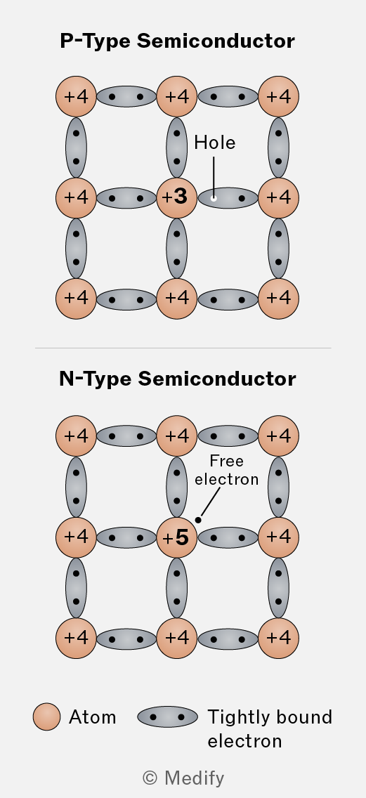
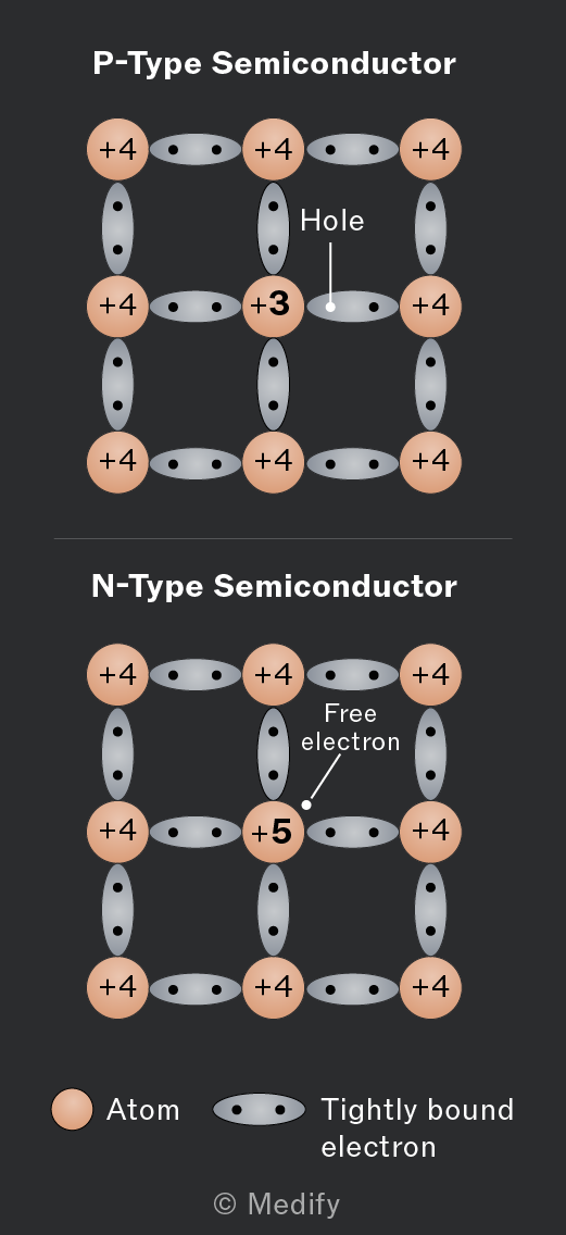
When a P-type and an N-type semiconductor are joined together, they form a diode. At the junction between the two, electrons from the N-side and holes from the P-side combine, creating a thin depletion region with no mobile charge carriers. This region acts like a barrier to current flow.
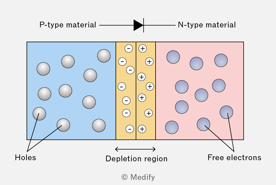
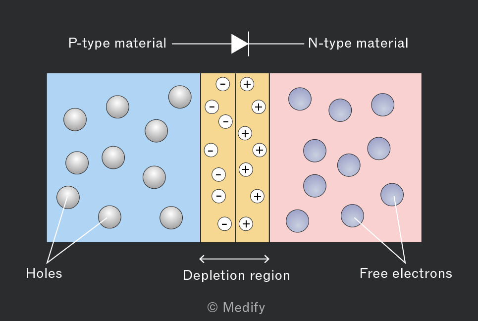
- If you connect the diode so that the positive voltage is on the P-side and the negative voltage is on the N-side (forward bias), the external voltage reduces the barrier, allowing electrons and holes to move across the junction and current to flow.
- If the diode is connected the other way around (in reverse bias), the barrier increases in size, and almost no current flows.
This one-way behaviour, which conducts in forward bias but blocks in reverse bias, is what makes diodes useful for controlling the direction of current in circuits.
A transistor is an electronic component that can act as a switch or an amplifier. It controls the flow of electric current using tiny changes in voltage. Instead of relying on moving parts like a mechanical switch, it operates through changes in how charge flows through semiconductor materials.
Transistors are constructed from regions of P-type and N-type semiconductors that are joined together. These junctions create barriers that can either block or allow the flow of charge depending on the applied voltages. By adjusting these voltages, the transistor can turn current on or off, or allow a small signal to control a much larger one.
Transistors are the building blocks of modern electronics. They form logic gates in computer chips, amplify sound in speakers, and switch power in circuits. Billions of them are packed into a single integrated circuit, but they all work using the same basic idea: a small electrical control manages a larger current.
A MOSFET (Metal Oxide Semiconductor Field Effect Transistor) is a type of transistor that uses an electric field to control how easily current can flow through a semiconductor channel.
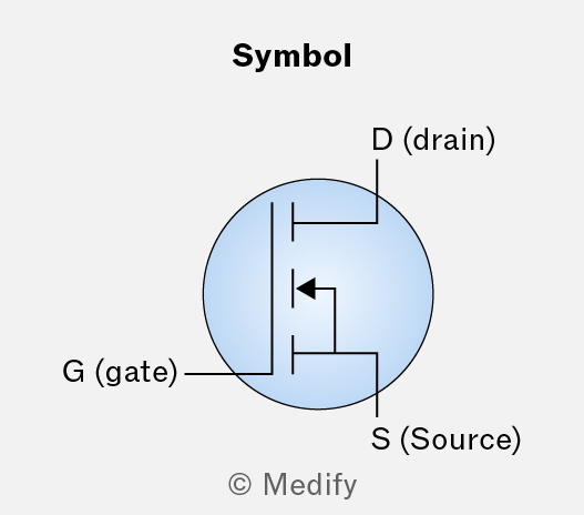
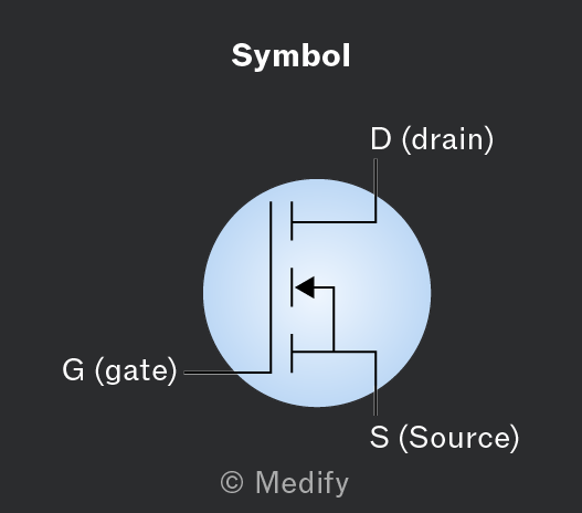
Below shows the circuit symbol for a MOSFET.
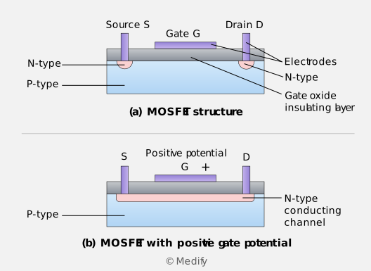
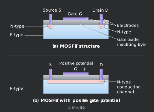
Its main body is made of P-type silicon, with two small N-type regions forming the source and drain.
The P-type channel prevents current flow when the MOSFET is switched off. Above this channel is the gate, a thin metal plate separated from the semiconductor by a very thin layer of silicon dioxide, which acts as an insulator.
To switch on a MOSFET, an input current must flow from the gate to the source. The resistance of the gate oxide layer (typically silicon dioxide) is so high that no current flows through. The gate then becomes positively charged (like the positive plate of a capacitor), creating an electric field in the semiconductor channel.
- The electric field attracts electrons from the N-type region towards the surface of the P-type region under the gate.
- When the voltage between the gate and the source, is high enough, a conductive path, known as an N-type conducting channel, forms between the drain and the source, so current can flow between them.
- The threshold voltage, where the n-type channel closes and the device switches off, is the gate–source voltage, . is generally between and
Because the MOSFET draws almost no current from the input circuit, it has a very high input resistance. This makes it highly energy efficient and ideal for use in integrated circuits and microchips.
Question walkthrough
Explaining N-channel MOSFET operation
Explains why the insulated gate of an N-channel enhancement MOSFET draws no current, and how a positive gate voltage forms a conducting channel between source and drain to switch it on.
The input characteristic curve illustrates how the drain current changes as the gate–source voltage increases.
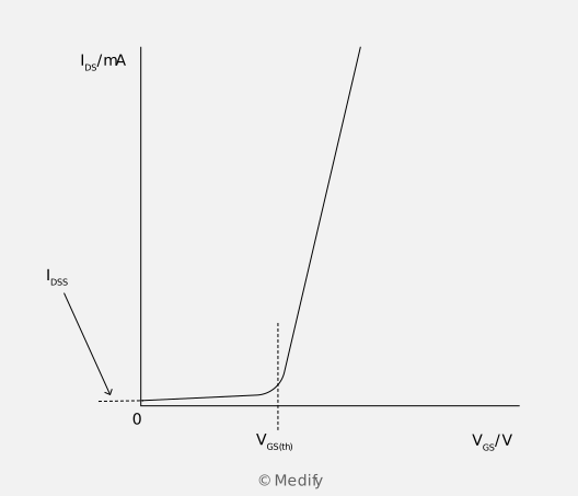
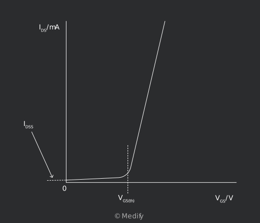
When is less than the threshold voltage almost no current flows. Once passes rises sharply as the MOSFET switches on.
The current that flows when is called the drain–source leakage
The output characteristic curves of a MOSFET show how the drain current changes with the drain–source voltage for different values of gate–source voltage
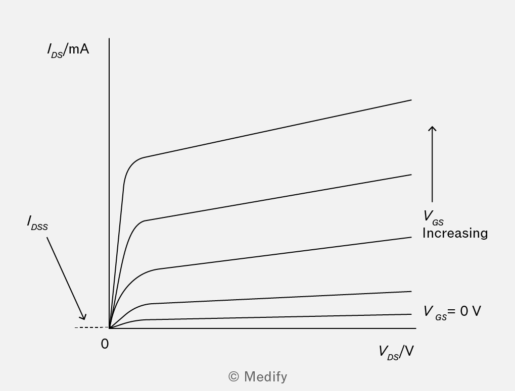
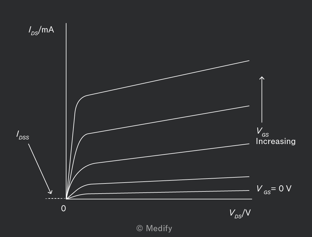
Each curve on the graph represents a fixed value. As increases, more current can flow because the electric field at the gate widens the conductive channel between the drain and source.
The lowest curve (for ) shows the very small current that flows
A MOSFET can act as an electronic switch, allowing a small logic signal to control a large current. In this circuit, a logic system controls the gate of the MOSFET.
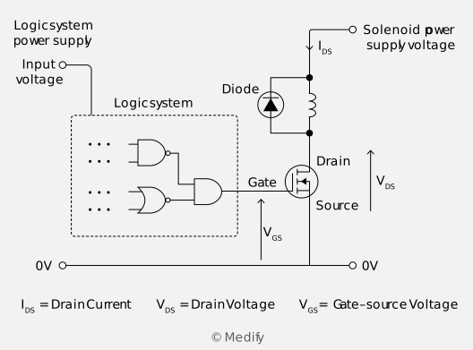
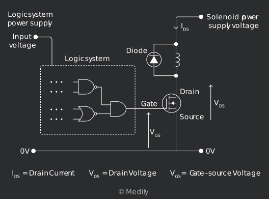
- When is greater than current flows from the drain to the source and powers the solenoid.
- When is less than or equal to no current flows, and the solenoid turns off.
When the MOSFET switches off, the current in the solenoid coil suddenly stops. Because coils store energy in their magnetic fields, Lenz’s law tells us that the coil will oppose this change by inducing a voltage that tries to keep the current flowing. This voltage can be very large and may damage the MOSFET. The diode across the solenoid provides a safe path for the current to flow until the magnetic energy is released, thereby protecting the transistor.
The gate of a MOSFET is insulated and draws almost no current, making it highly resistive. As a result, it can easily pick up a small electric charge from its surroundings. If the gate is left unconnected, stray charges can cause the MOSFET to switch on or off randomly.
To prevent this, a resistor, is connected between the gate and This provides a safe path for the charge to leak away, keeping the gate at a definite voltage when no input signal is present.
The value of is chosen to be large, approximately so that it keeps the gate stable without affecting the input signal.
Question walkthrough
Finding voltage across a MOSFET switch
Uses the total series resistance to find the circuit current, then V=IR to find the small voltage drop across a fully-on MOSFET switching a motor.
A Zener diode is a type of diode designed to work in reverse. The circuit symbol for a Zener diode is illustrated below.
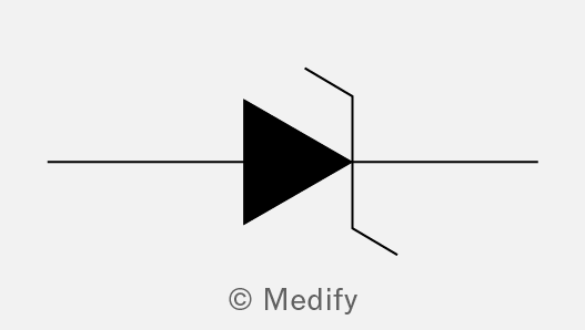
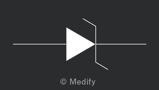
In a normal diode, current flows only when it is forward-biased, and reverse voltage stops the current. A Zener diode is designed so that when the reverse voltage reaches a certain threshold, called the Zener breakdown voltage, current starts flowing steadily in the reverse direction without damaging the diode.
This property makes it very useful for voltage regulation. As long as the current through the diode stays above a small minimum value, the voltage across it stays almost constant at This allows a Zener diode to act as a stable voltage reference in circuits.
The I–V characteristic of a Zener diode looks similar to that of a normal diode in the forward bias direction. Both conduct once the forward voltage reaches approximately 0.3 to 0.7 V (for silicon diodes).
It is important to note that the primary difference is evident in reverse bias. For a normal diode, almost no current flows until the reverse breakdown voltage is reached, typically 50 to 400 V, which can permanently damage it.
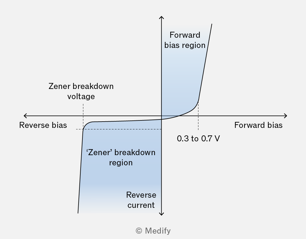
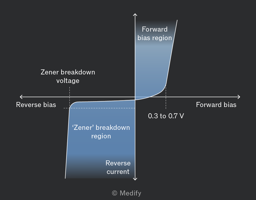
A Zener diode, however, is designed so that reverse breakdown occurs safely at a much lower, controlled voltage known as the Zener breakdown voltage.
In this Zener breakdown region, the voltage across the diode remains nearly constant even as the current varies. This makes Zener diodes very useful for voltage regulation, reference circuits, and overvoltage protection.
When a Zener diode is used as a voltage regulator, it is connected in reverse bias in series with a resistor.
- When the input voltage is less than the Zener voltage, the current in the circuit is zero.
- When the input voltage is greater than or equal to the current in the circuit is non-zero.
For a Zener diode, the voltage across it changes very little over a wide range of currents. Therefore, once the input voltage exceeds the voltage across the diode remains approximately constant.
A load can be connected in parallel with the Zener diode (between the terminals in the diagram). Since the load shares the same two circuit points, it experiences the same constant voltage, allowing the Zener diode to maintain a steady load voltage even when the supply voltage varies.
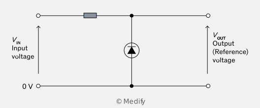
The load resistance must be significantly higher than the dynamic resistance of the Zener diode, allowing the load to draw negligible current. This allows almost all the current to flow through the Zener diode, meaning the series resistor and Zener can be treated as a potential divider.
For the Zener diode to regulate properly, the current through it must be greater than the minimum Zener current, but not exceed the maximum rated value. This ensures the voltag across the diode and the load remains constant.
Question walkthrough
Finding current through a Zener diode
Uses the voltage across the series resistor and Kirchhoff’s current law to find the current through a Zener diode in a voltage regulator circuit, given the load current.
A photodiode is a special type of p–n junction diode designed to convert light into electrical current.
- When light strikes the junction, photons are absorbed and release charge carriers, creating a photocurrent.
- This light-generated effect occurs in all p–n junctions, which is why normal diodes and transistors are sealed to keep out light.
- In a photodiode, the junction is deliberately exposed using a transparent window or lens to capture light.
Below shows the circuit symbol for a photodiode:
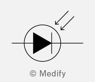

A solar cell is simply a photodiode with a large exposed junction, or an array of junctions, designed to maximise light collection and electrical output.
In a photodiode, the photocurrent increases with light intensity. The graph below shows how photocurrent varies with light intensity for a typical photodiode.
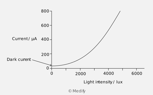
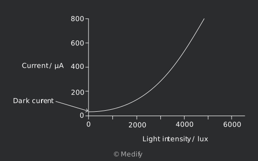
Even in complete darkness, a very small current flows through the photodiode. This is the dark current, typically
The responsivity of a photodiode indicates the amount of current produced for a given light power. A common value is around Higher responsivity gives a greater electrical current for the same light power.
Photodiodes can be used in two main modes: photovoltaic and photoconductive.
- In photovoltaic mode, no external voltage is applied, and the photodiode generates a voltage in response to light. This is how solar cells operate.
- In photoconductive mode, the photodiode is reverse-biased.
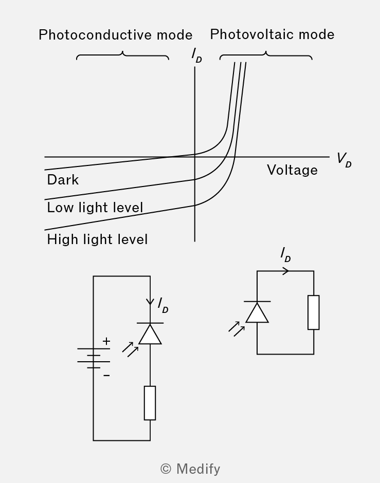
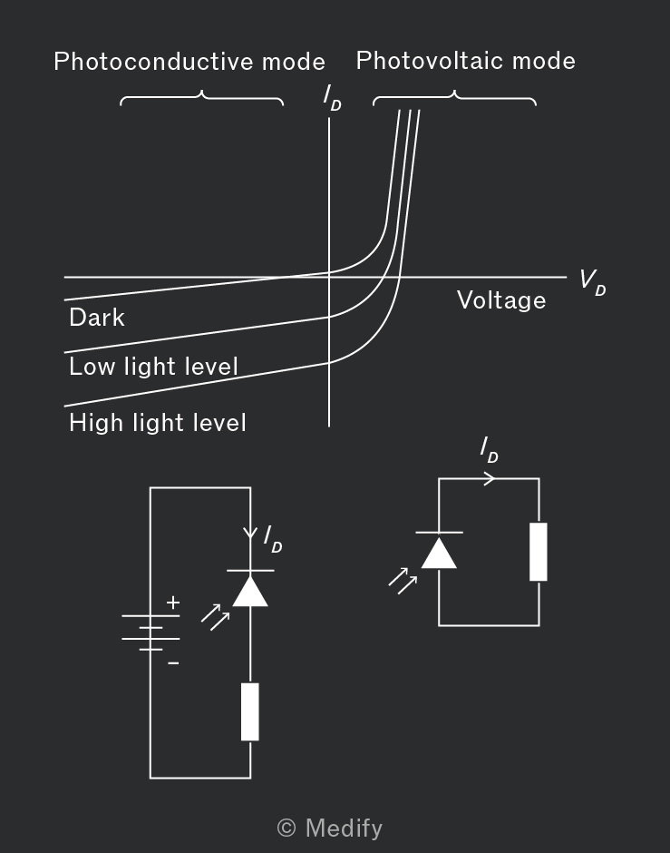
A reverse–bias voltage creates a stronger electric field across the p–n junction. This field pulls electrons and holes away from the junction, exposing more fixed ions. As a result, the depletion region widens, which improves the diode’s sensitivity and reduces its response time.
Photoconductive mode is commonly used because:
- the photocurrent changes very linearly with light intensity,
- sensitivity increases with reverse bias, and
- the response time is much faster than in photovoltaic mode.
Different photodiodes are designed to detect different wavelengths of light, from infrared to ultraviolet.
A spectral response curve illustrates the sensitivity of a device across its wavelength range.
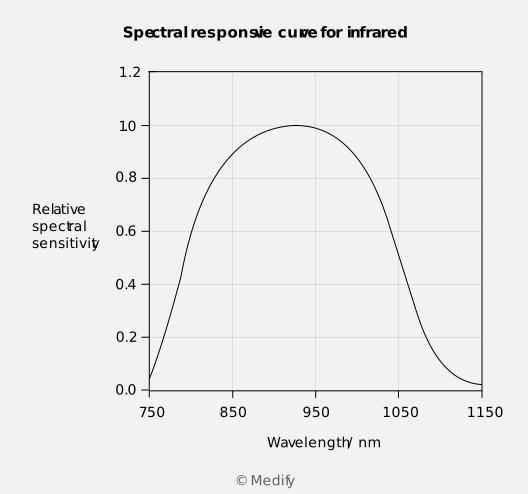
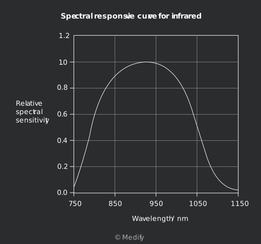
Infrared photodiodes are widely used in optical fibre receivers, where they detect the light pulses transmitted along the fibre. Their sensitivity and fast response make them ideal for high-speed communication systems.
The Hall effect is the production of a small voltage across a current-carrying conductor or semiconductor when it is placed in a magnetic field.
A Hall-effect sensor, shown below, uses the Hall effect to detect a magnetic field.
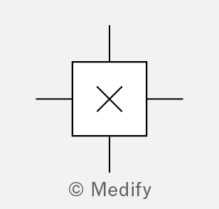

Inside the sensor, a thin semiconductor carries a steady current. When a magnetic field is present, the resulting Hall voltage is measured by the electronics in the device. This voltage changes in proportion to the magnitude and direction of the magnetic field.
Hall effect sensors are used to detect proximity, speed, and position by sensing magnetic fields, enabling a wide range of applications. Examples of this include:
- automotive systems like anti-lock brakes and speedometers,
- consumer electronics, such as brushless DC motor controllers, and
- smartphone compasses (as hall effect sensors can be sensitive enough to detect the Earth’s magnetic field).
A Hall effect sensor can detect the motion of a rotating part in an engine. A small magnet is attached to the rotating component.
Each time the magnet passes the sensor, the magnetic field at the sensor increases in strength. This produces a pulse of Hall voltage. The faster the component rotates, the more pulses per second the sensor produces. A Hall effect sensor for a vehicle is shown below:
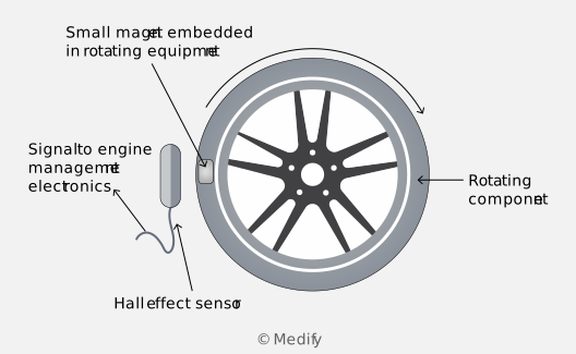
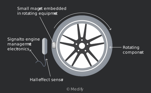
The stream of pulses is sent to the engine management electronics. By measuring the frequency of these pulses, the system can calculate the rotational speed.
This information is crucial for precisely controlling fuel injection, ignition timing, and other engine functions.
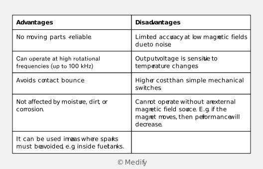
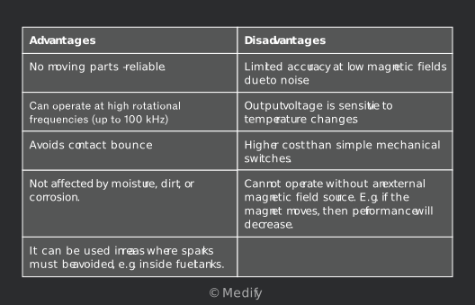
The table below gives some advantages and disadvantages of Hall effect sensors.
Question walkthrough
Explaining Hall effect speed sensing
Explains how a Hall effect sensor detects a rotating magnet passing it once per revolution, producing a voltage pulse that is counted each second to determine rotational speed.