
Operational amplifier in (3.13.4)
On this page
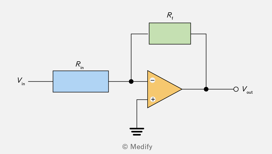
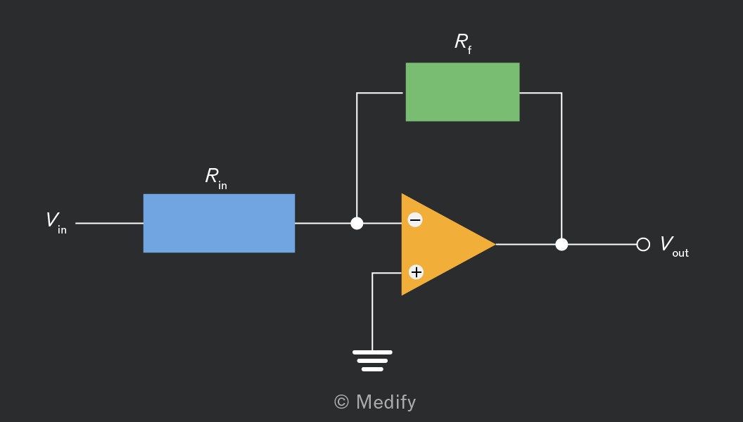
In an inverting amplifier configuration, the operational amplifier’s output voltage is fed back into its inverting input.
This forms a closed-loop negative feedback circuit, allowing the operational amplifier’s gain to reach much lower values.
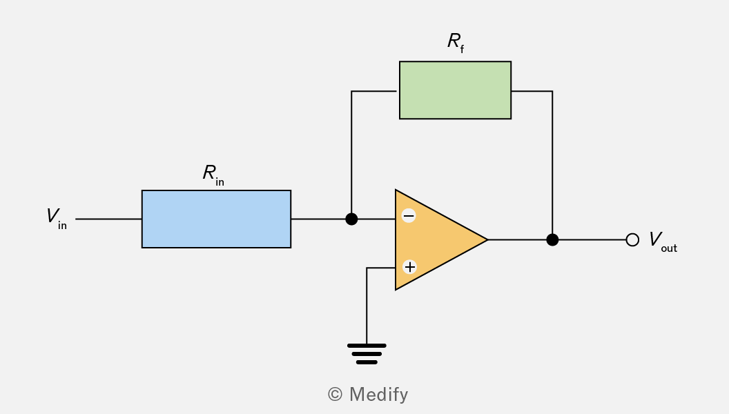
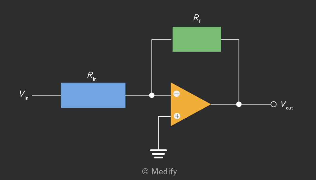
The output voltage equation is known as the transfer function, and with two assumptions, we can derive an expression for it using virtual-earth analysis:
- The operational amplifier can be considered ideal, meaning it has infinite open-loop gain,
- The operational amplifier is not saturated, (the magnitude must be less than the supply voltage), meaning it is operating in its linear region.
The diagram shows that the non-inverting input voltage is connected to ground and therefore must be at 0 V.
Substituting these two assumptions into the open-loop transfer function gives:
Rearrange this to make the subject:
This result proves that the voltage at is also at 0 V, even though it is not physically connected to earth.
A point in a circuit with a voltage of 0 V, even though it is not connected to earth, is known as a virtual earth.
Virtual earth is useful in circuit analysis because it provides a reference potential.
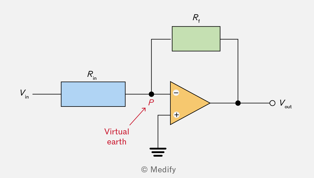
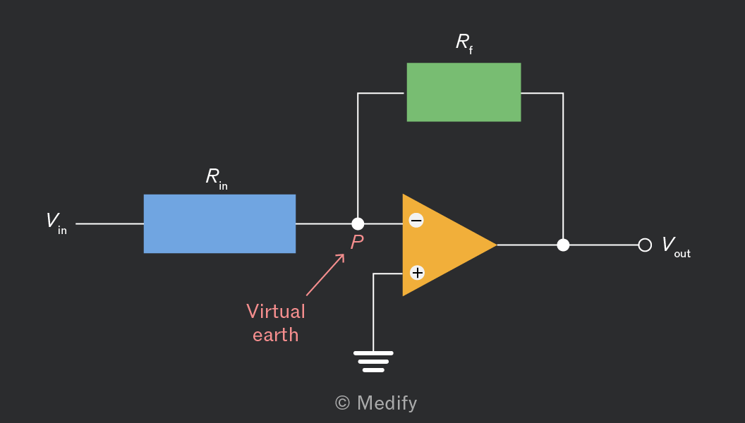
The circuit diagram illustrated below contains a virtual earth.
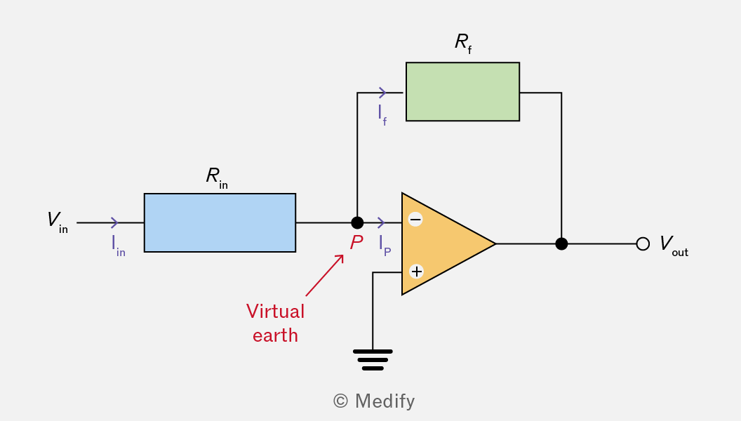
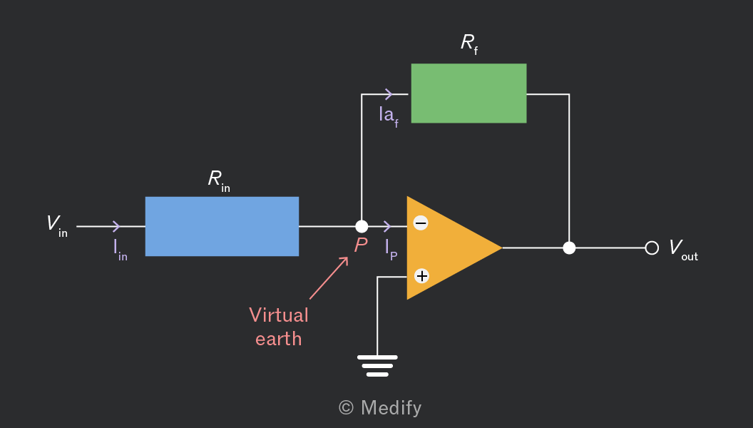
Derivation of the transfer function can be broken down into the following steps:
1. The input resistance is infinite because the operational amplifier is ideal. If the resistance is infinite, there is no current, and Real op-amps have small bias currents.
2. Using Kirchhoff’s current law, it is clear that the current passing through is the same as the current passing through
3. Ohm’s law can be used to provide expressions for the current through the resistors:
4. As these currents are equal, we can equate the two expressions and make the subject:
5. Applying Kirchhoff’s voltage law to the loop involving and gives the following expression:
6. Substitute the expression in step 4 into this equation and rearrange to get the transfer function:
Question walkthrough
Calculating inverting amplifier output voltage
Converts millivolt and kilohm/megohm values to standard form, then applies V_out = −(R_f/R_in)×V_in to find the output voltage of an inverting operational amplifier circuit.
Question walkthrough
Finding inverting amplifier input voltage
Rearranges the transfer equation V_out/V_in = −R_f/R_in to find the input voltage of an inverting operational amplifier from a given output voltage and feedback/input resistor values.
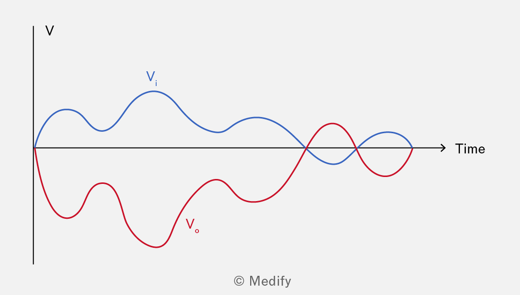
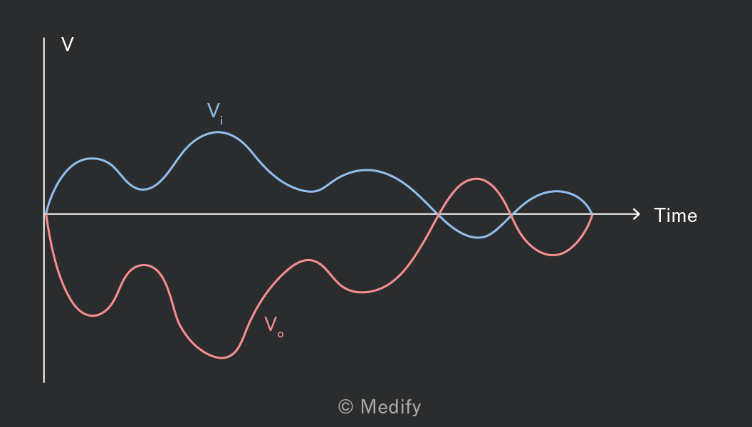
An inverting amplifier amplifies the input voltage and reverses (inverts) the signal polarity.
This can be shown clearly by plotting the input voltage, and the output voltage, on a voltage–time graph.
The input signal of an inverting amplifier configuration typically exhibits lower distortion than that of a non-inverting configuration.
If it is important that the signal’s original polarity does not change, a non-inverting amplifier configuration can be used instead.
In this configuration, the operational amplifier’s output feeds back into its input. As with the inverting amplifier configuration, this creates a closed-loop circuit with negative feedback.
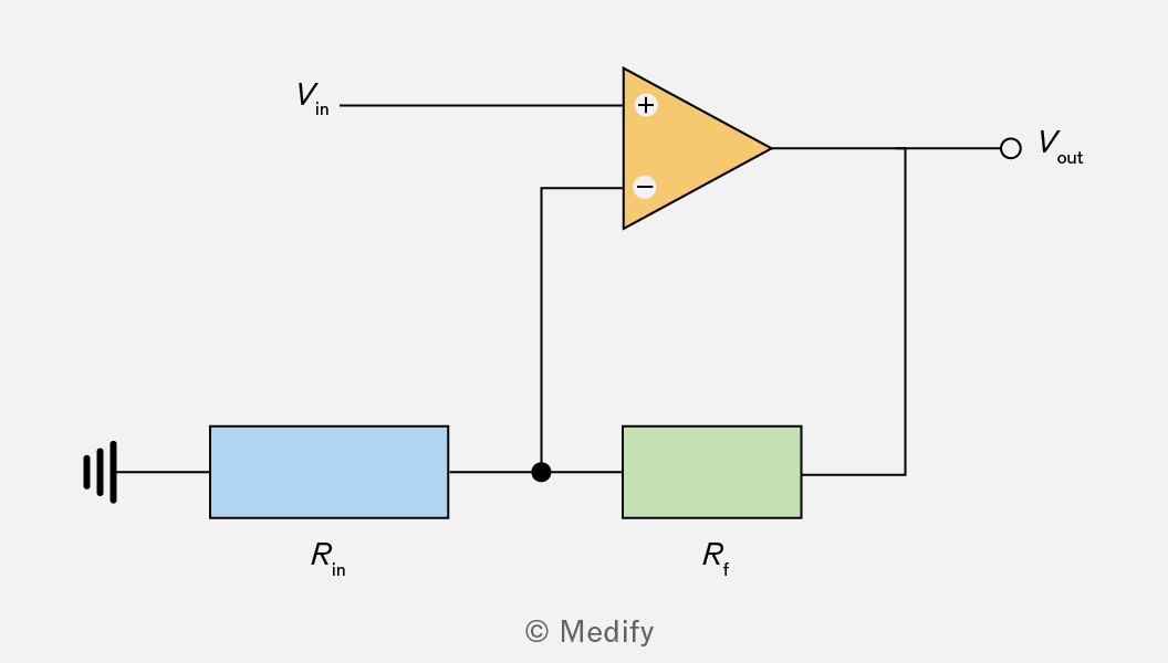
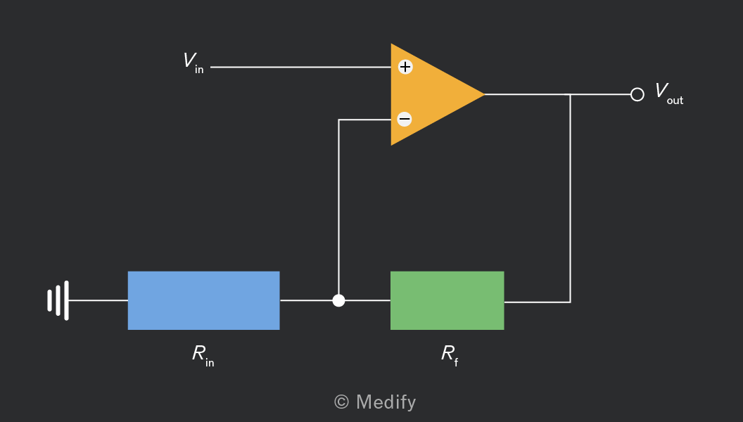
The gain of a non-inverting amplifier configuration has a minimum value of one as seen by the transfer function:
In this configuration, the input signal is directly connected to the operational amplifier. The operational amplifier has infinite input resistance, so the entire circuit draws no current.
This is an advantage of the inverting operational amplifier: it draws current through
Question walkthrough
Finding input resistance for non-inverting amplifier
Rearranges the non-inverting amplifier gain formula (V_out/V_in = 1 + R_f/R_in) to find the input resistor value from a given gain and feedback resistor.
It is easy to get confused between inverting and non-inverting amplifiers. Both configurations use an operational amplifier with feedback, but the gain equations are different, and the inverting amplifier introduces a negative sign.
Keeping track of the sign and the correct formula for each configuration will help you avoid common calculation errors.
In certain situations, a unity gain buffer is formed. A unity gain buffer is a circuit with no amplification, or in other words, a gain of one.
For this to happen, either the resistance of must be infinite, or the resistance of must be zero. This effectively forms the circuit below:
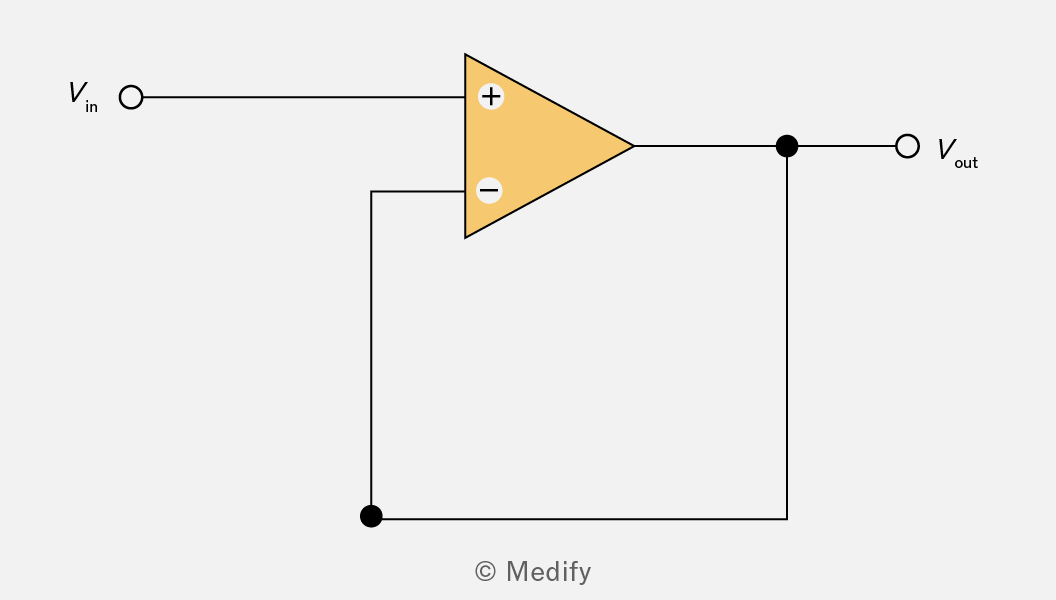
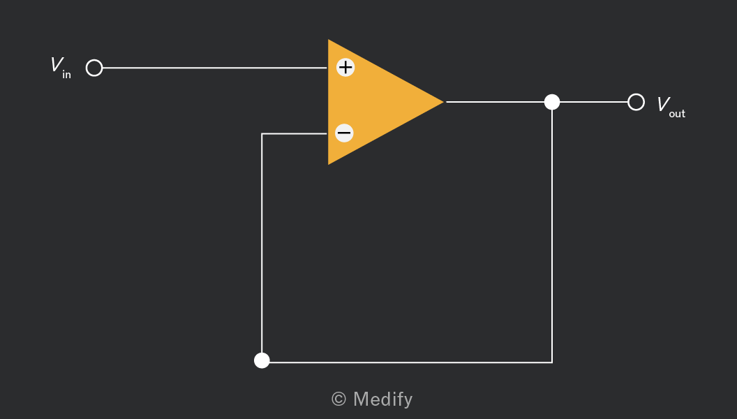
Unity gain buffers are useful as an interface between devices with low input resistance and an input signal. They do not disturb the original circuit, but they will output the same input signal and draw no current.
A summing amplifier configuration can be used when multiple signals are present. This configuration allows each signal to be amplified independently, even though they are all connected to the inverting amplifier. This is due to the virtual earth, which prevents any interference between the signals.
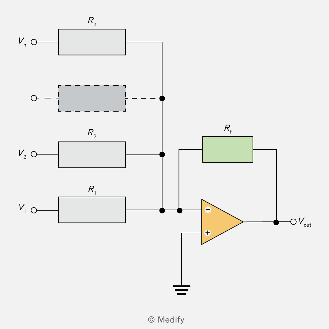
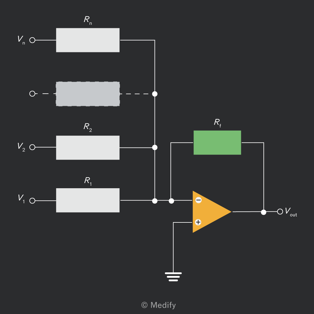
The transfer function is given by:
Audio mixers use a summing amplifier configuration so that different audio signals can be input and merged whilst still enabling the individual signals to be amplified independently.
Question walkthrough
Finding feedback resistance in summing amplifier
Uses the summing-amplifier transfer function V_out = −R_f(V₁/R₁+V₂/R₂+V₃/R₃) to find the feedback resistor value from three equal input voltages, their input resistors, and the output voltage.
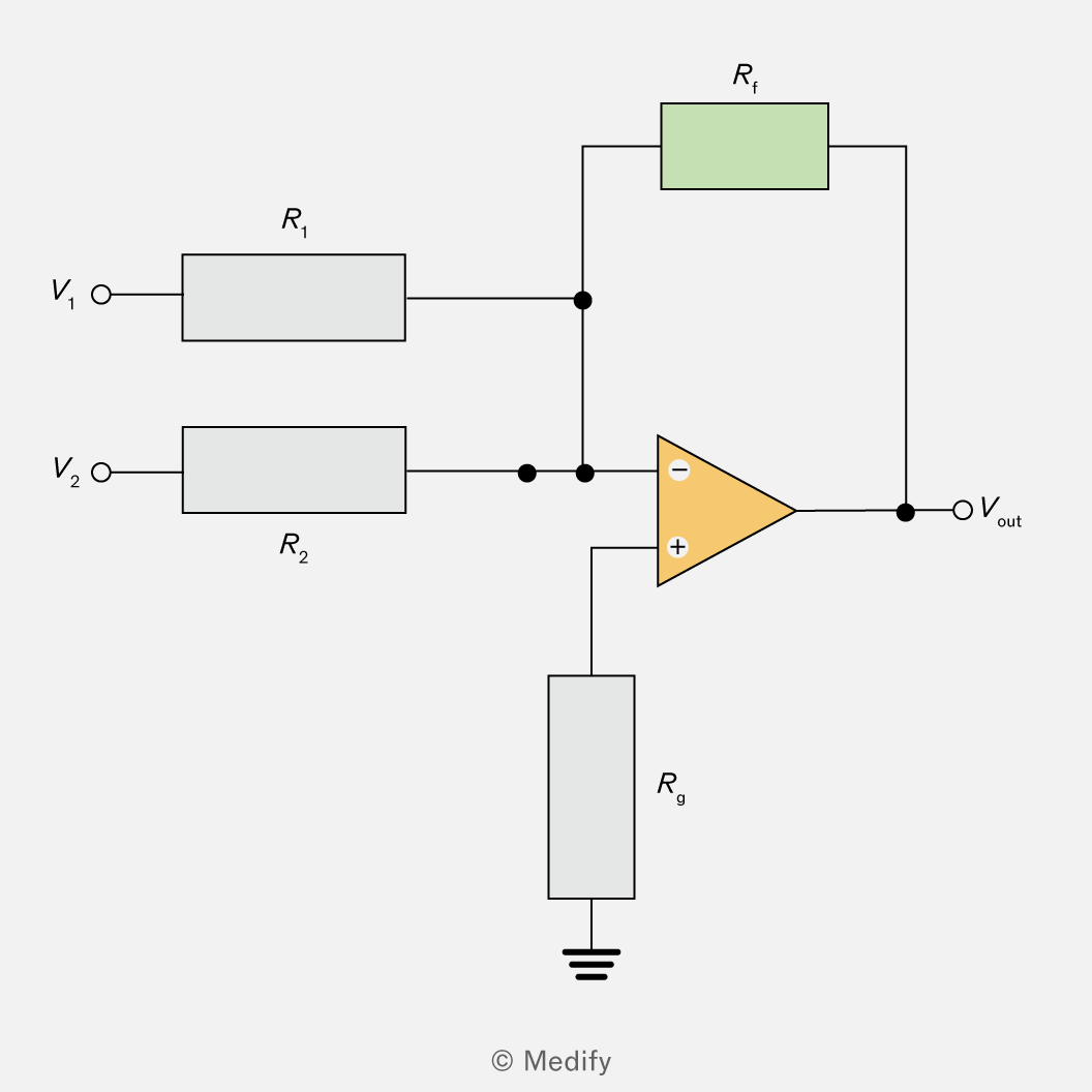
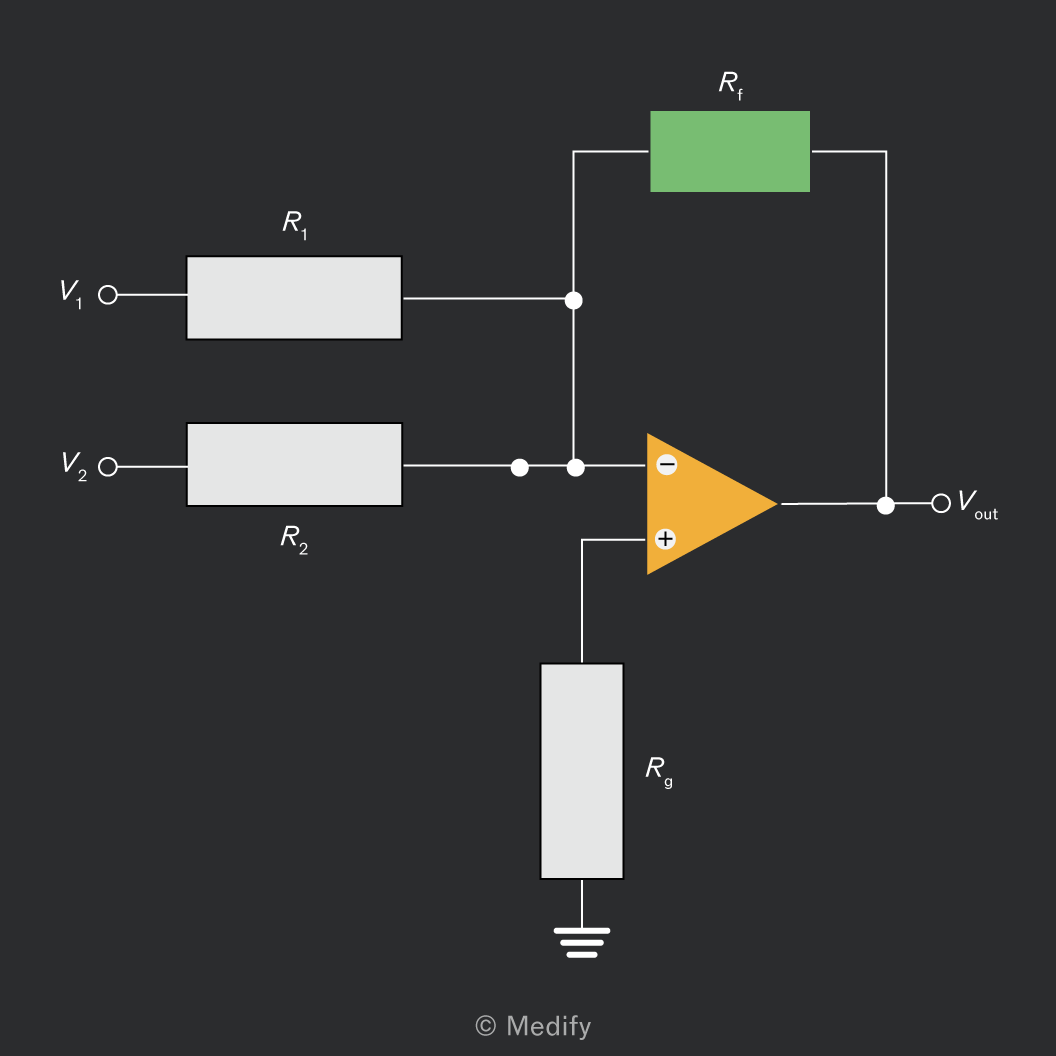
A difference amplifier configuration calculates the difference between two signals and subtracts it from the original signals.
Most uses of this configuration require the gains of both signal inputs to be the same. For this to be the case, must be equal to and must be equal to
The transfer function for this circuit is:
Question walkthrough
Finding difference amplifier output voltage
Applies the difference-amplifier transfer function V_out = (V₊ − V₋)(R_f/R₁) to find the output voltage from two input voltages and the input/feedback resistor values.
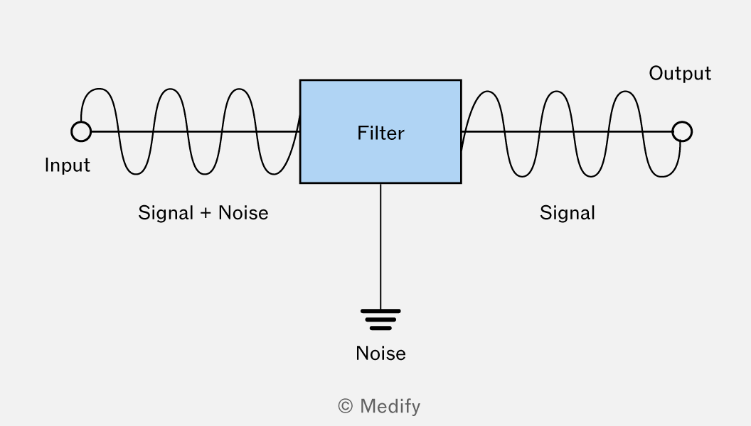
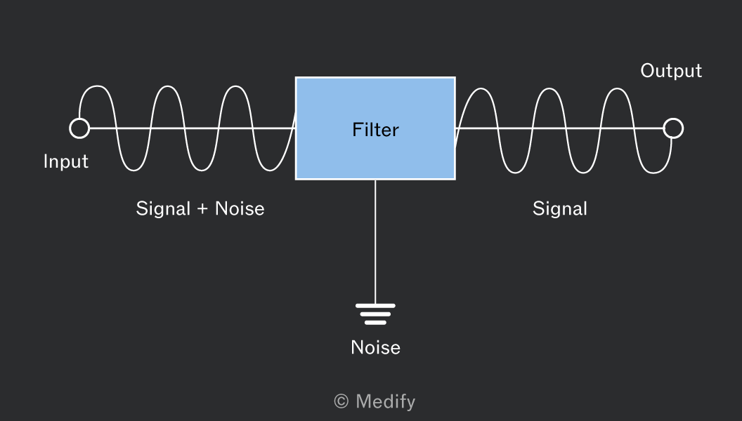
A common use of a difference amplifier is noise cancellation. A couple of examples of this are outlined below:
Microphones are often affected by interference due to the mains electricity at 50 Hz. If all 50 Hz signals were filtered out, this would also remove any parts of the original signal at
50 Hz. However, using a difference amplifier allows both the original signal and an inverted signal as inputs. When these signals are subtracted, the interference is cancelled out.
An electrocardiogram (ECG) measures the potential differences generated by the heart. Electrodes are attached to the body for this measurement. Because this measurement is extremely sensitive, the leads frequently pick up interference from the mains electricity.
This interference is removed using a difference amplifier and an extra electrode. This additional electrode is typically placed far from the heart, often on the ankle. Since its signal is primarily caused by interference, the difference amplifier can use it to cancel out the unwanted signal from the main measurement.
Real operational amplifiers are not ideal, although their performance is optimised for their particular application. For example, factors such as temperature of the environment in which they operate will also impact their performance.
| Ideal | Real | |
|---|---|---|
| Open-loop gain | Infinite | 106 |
| Input resistance | Infinite (draws no current) | 1012 |
| Output resistance | Zero | |
| Output voltage | |
|
| Bandwidth | Operates at any input frequency (infinite bandwidth) | Typical open loop: Typical closed loop: |
The differences between real and ideal operational amplifiers will affect their operations in the following ways:
- Input resistance is not infinite, and therefore, a current will be drawn. This is very small (typically nA) due to the high resistance.
- The output resistance is higher than that of an ideal amplifier, limiting the current it can deliver.
- In a negative feedback circuit, the output resistance is reduced.
The open-loop gain of a real operational amplifier is still extremely high, and it is a reasonable assumption to take it as infinite.
An ideal operational amplifier has an output voltage of 0 V when the inverting and non-inverting terminals are the same. However, this is not true for a real operational amplifier. A real operational amplifier has a small output voltage (the offset voltage).
The offset voltage must be cancelled out using the ‘Offset Null’ pin connection, which connects the operational amplifier to an external potential divider circuit.
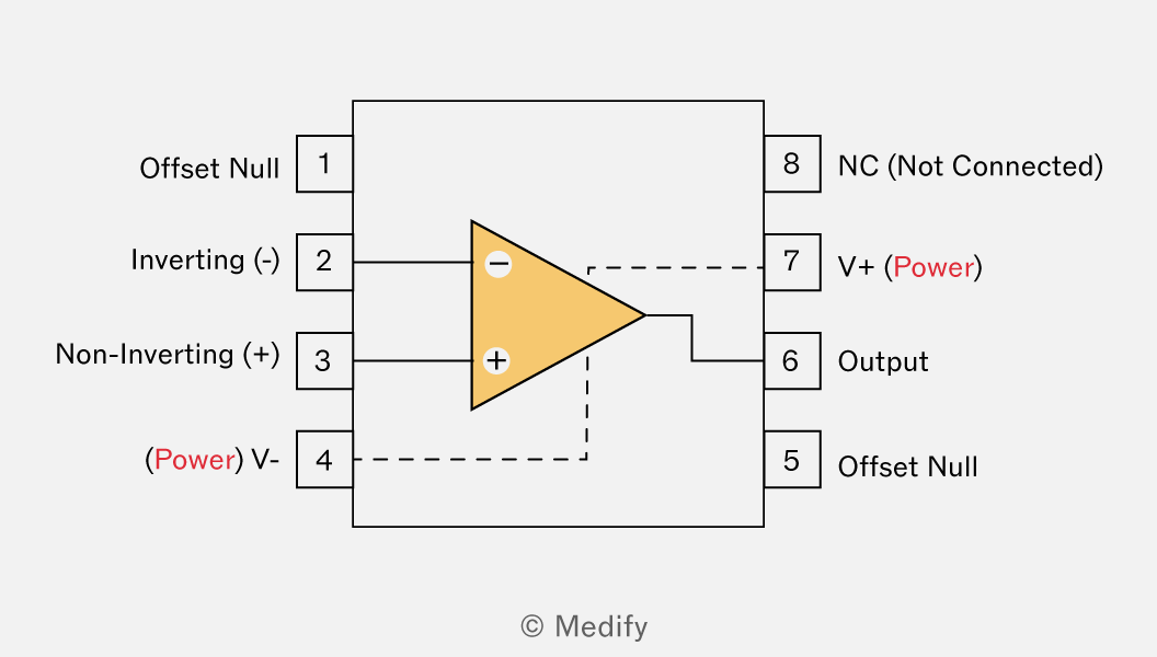
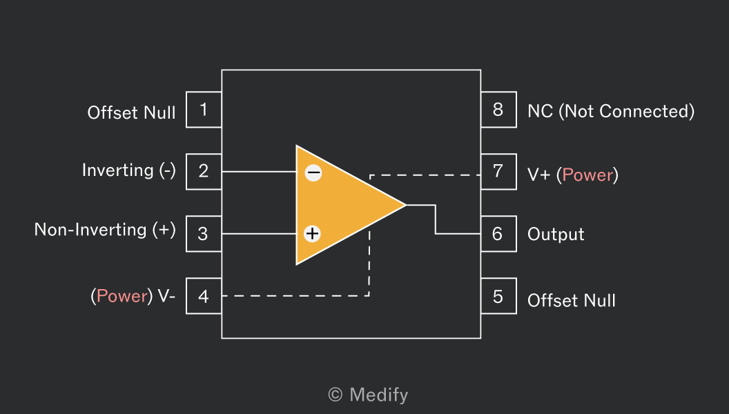
In a real operational amplifier, there is always some power loss due to resistance in the circuit itself and voltage drops across internal transistors and protection circuitry, meaning the output voltage is not equal to the supply voltage.
We can illustrate how the voltage gain of an operational amplifier varies with the input signal frequency using a frequency response curve.
It is important to note that gain and frequency often have large values, so these curves can be plotted on logarithmic rather than linear scales.
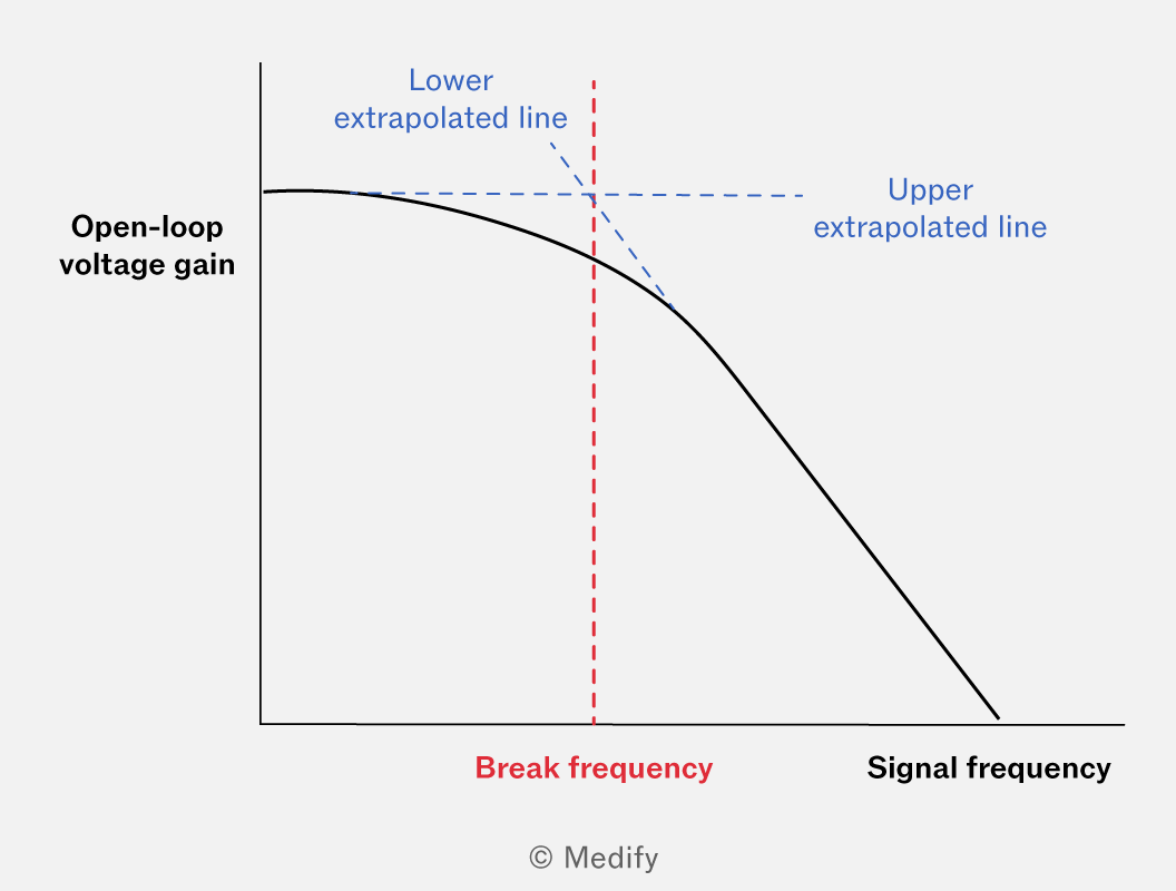
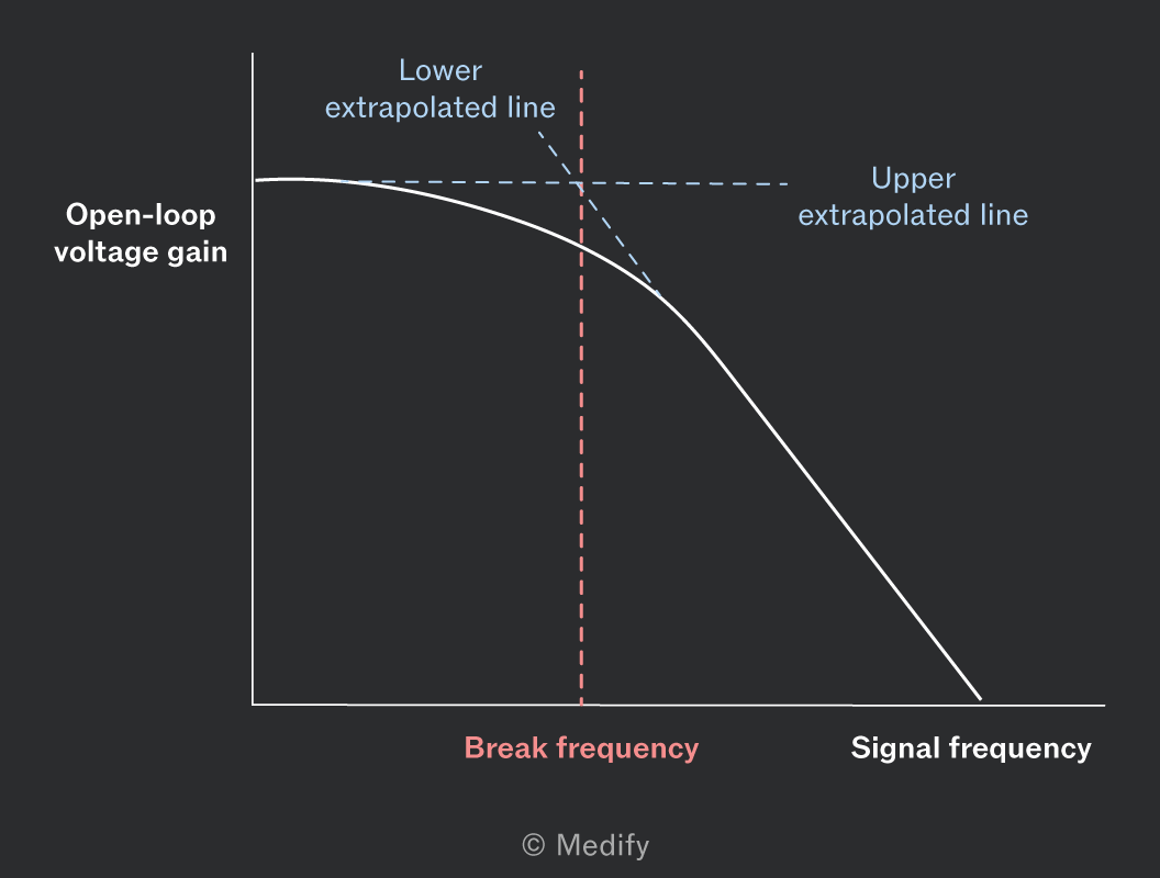
Break frequency is defined as the frequency at which the gain begins to change.
Break frequency is the point of intersection of the two linear sections of the graph and can be found by extrapolating the lines.
In an open-loop circuit, the frequency response curve shows that above the break frequency, the operational amplifier’s performance decreases rapidly.
This performance issue can be overcome by using the operational amplifier in a closed-loop circuit. This increases the break frequency’s value.
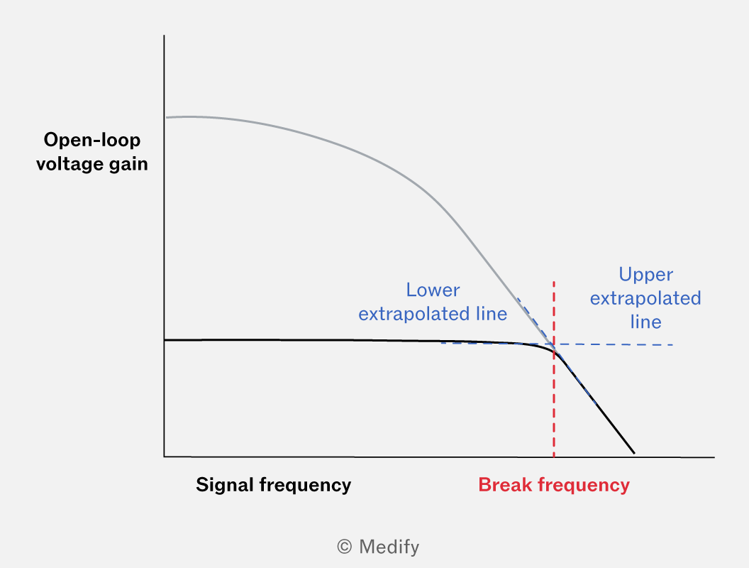
At frequencies above the break frequency, the relationship between gain and bandwidth is linear, as shown by the graph.
Mathematically, this can be written as:
This can be used to predict the circuit bandwidth for a given operational amplifier.
Ideal operational amplifiers are theoretical and describe perfect operating conditions. In reality, these conditions are never achieved.